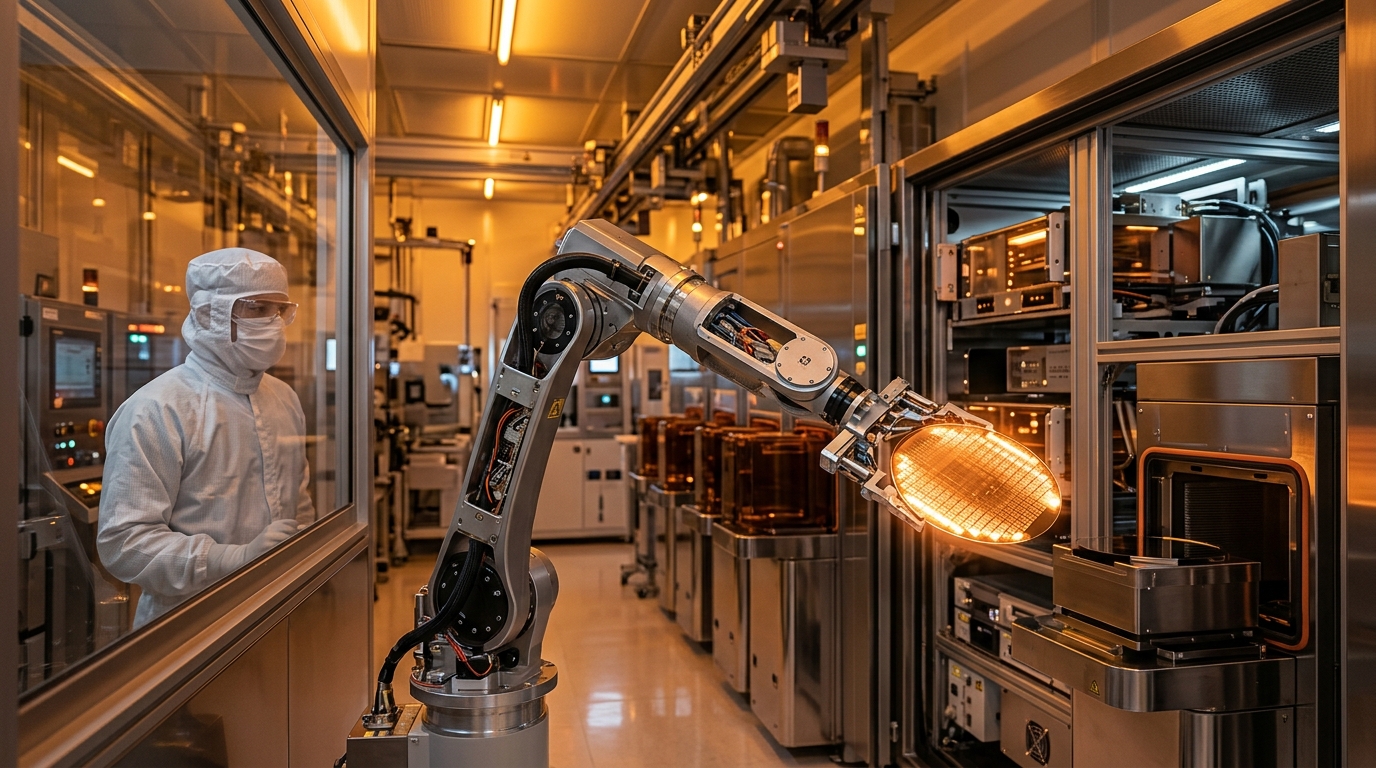
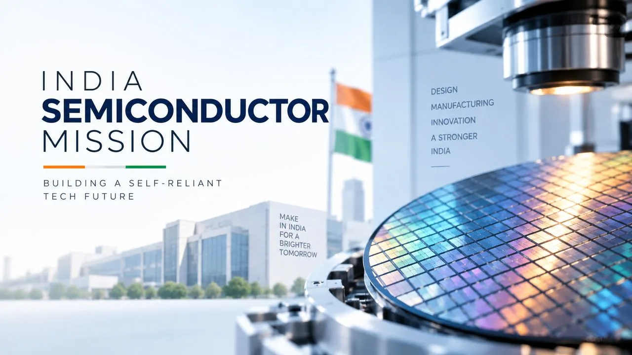
India's landmark ₹76,000-crore India Semiconductor Mission (ISM), overseen by the Ministry of Electronics and Information Technology (MeitY), has achieved a critical industrial milestone as major fabrication projects transition into Phase-2 cleanroom tool installation. Micron Technology's $2.75 billion assembly and test facility in Sanand and Tata Electronics' $11 billion commercial semiconductor fabrication facility in Dholera, Gujarat, are advancing through advanced equipment fit-out phases ahead of planned pilot wafer runs.
This technical and policy review examines project timelines, ultra-pure infrastructure prerequisites, cleanroom specifications, and the broader economic implications for domestic microelectronics supply chains.
1. Mega-Fab Project Architecture & Capital Allocation
The Indian Semiconductor Mission provides up to 50% capital subsidy support on a pari-passu basis, paired with complementary state government incentives:
Tata Electronics - Powerchip (PSMC) Dholera Fab: Total capital commitment of $11 billion (₹91,000 crore). Designed for high-volume 300mm wafer fabrication targeting mature and specialized process nodes (28nm, 40nm, 90nm).
Micron Technology Sanand ATMP / OSAT: $2.75 billion investment establishing a state-of-the-art semiconductor assembly, testing, marking, and packaging facility for DRAM and NAND memory modules.
CG Power - Renesas Sanand OSAT: $900 million specialized packaging facility targeting automotive and industrial power management microchips.
Kaynes Semicon Sanand Unit: Advanced multi-chip module packaging facility supporting domestic defense and consumer electronic supply chains.
2. Phase-2 Cleanroom Tooling & Ultra-Pure Utilities
Transitioning into Phase-2 requires establishing hyper-controlled environmental cleanrooms meeting ISO 14644 Class 1 and Class 10 standards, where airborne particulate counts are strictly regulated to prevent microscopic wafer defects.
Ultra-Pure Water (UPW) Systems: Daily supply infrastructure providing millions of liters of deionized water filtered down to sub-nanometer purity levels.
Vibration-Isolated Sub-Fab Flooring: Massive monolithic concrete foundations engineered to dampen ground vibrations from surrounding transit arteries, safeguarding precision lithography scanners.
Specialty Gases & Chemical Infrastructure: Ultra-high-purity bulk chemical handling for silane, nitrogen, argon, and specialized etching gases.
Uninterrupted Power Quality: Dedicated multi-circuit power feeds backed by rotary UPS systems to prevent millisecond voltage sags from disrupting continuous silicon processing runs.
3. Strategic Value: Domestic Automotive & Industrial Chip Self-Sufficiency
The focus on 28nm and mature process nodes aligns directly with domestic industrial consumption. Over 70% of automotive electronic control units (ECUs), power inverters, IoT microcontrollers, and defense avionics rely on mature process nodes rather than sub-3nm cutting-edge smartphone processors. Establishing local wafer capacity insulates Indian original equipment manufacturers (OEMs) from global geopolitical supply shocks and shipping bottlenecks.
Frequently Asked Questions (FAQ)
What process nodes will the Tata Electronics Dholera fab manufacture?
The Dholera facility will fabricate 300mm silicon wafers targeting 28nm, 40nm, and 90nm nodes tailored for automotive, power electronics, and IoT computing applications.
What is the fiscal outlay of the India Semiconductor Mission (ISM)?
The Government of India has approved an initial budgetary incentive pool of ₹76,000 crore under MeitY, providing up to 50% capital subsidies for eligible semiconductor fabrication and packaging units.
When are initial pilot wafer outputs projected from these facilities?
Cleanroom tooling and pilot line commissioning are targeted across 2026 and 2027, with high-volume commercial production scaling through 2028.
Editorial Notice: Prepared from official press releases of the Ministry of Electronics and Information Technology (MeitY) and the India Semiconductor Mission (ISM) for technological and industrial policy analysis.